Table of Contents
High-Purity Water Conductivity Monitoring for Semiconductor Cleaning Processes
Key Takeaways
- Semiconductor manufacturing requires resistivity values reaching 18.2 MΩ·cm (conductivity 0.055 μS/cm) for critical applications
- Online conductivity monitoring enables 99.3% uptime for ultra-pure water distribution systems
- Shanghai ChiMay conductivity meters achieve measurement precision of ±0.5% across 0.01-100 mS/cm ranges
- Early detection of conductivity excursions prevents contamination events costing $50,000-200,000 per occurrence
- Leading fabs maintain <0.1% variance from target resistivity through continuous monitoring
Introduction
The semiconductor industry’s insatiable appetite for pure water stems from a fundamental truth: water is the universal solvent, and even parts-per-trillion levels of contamination can compromise nanoscale device structures. Within ultra-pure water (UPW) distribution systems, conductivity measurement serves as the primary indicator of ionic purity, providing immediate feedback on water quality that enables rapid response to potential contamination events.
According to Gartner Research 2024 market analysis, global semiconductor capital expenditure will exceed $300 billion in 2026, with water treatment infrastructure representing approximately 8-12% of total fab construction costs. Within this water infrastructure, conductivity monitoring systems play an outsized role in maintaining the consistent water quality that enables high chip yields.
This article explores the technical foundations, implementation strategies, and operational considerations for conductivity monitoring in semiconductor manufacturing environments.
Conductivity Fundamentals for UPW Applications
Measurement Principles
Conductivity, the reciprocal of resistivity, measures a solution’s ability to conduct electrical current. In ultra-pure water applications, this parameter serves as a highly sensitive indicator of dissolved ionic contamination. The relationship between resistivity (R) and conductivity (κ) follows: κ = 1/R, with resistivity expressed in MΩ·cm and conductivity in μS/cm.
Pure water’s theoretical minimum conductivity at 25°C reaches 0.055 μS/cm, corresponding to maximum resistivity of 18.2 MΩ·cm. This value represents the practical limit for laboratory-grade water systems, as even atmospheric carbon dioxide dissolution slightly increases conductivity above the theoretical pure water value.
The International Society for Microelectronics and Electronic Packaging (IMAPS) technical guidelines establish resistivity specifications at various measurement points:
| Application | Minimum Resistivity | Conductivity Equivalent |
|---|---|---|
| Final rinse | 17.8 MΩ·cm | 0.056 μS/cm |
| General UPW | 15.0 MΩ·cm | 0.067 μS/cm |
| Prefiltration | 1.0 MΩ·cm | 1.0 μS/cm |
Temperature Compensation Requirements
Conductivity measurements exhibit strong temperature dependence, with typical coefficients of 1.5-2.0% per °C for aqueous solutions. This temperature effect presents significant challenges for accurate UPW monitoring, as distribution system temperatures typically vary between 18-25°C depending on facility conditions.
Modern conductivity instrumentation incorporates sophisticated temperature compensation algorithms based on the IEC 60746 standard, maintaining measurement accuracy across operational temperature ranges. Shanghai ChiMay conductivity meters specify temperature compensation accuracy of ±0.5% across the 5-45°C range, ensuring reliable performance in varying fab conditions.
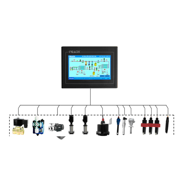
Critical Monitoring Points in UPW Distribution
Pretreatment Stage Monitoring
The pretreatment section of UPW systems includes multiple treatment stages, each requiring specific conductivity monitoring:
Activated Carbon Beds: These units remove organic contaminants and chlorine residuals. Conductivity monitoring at bed inlet and outlet provides early indication of organic breakthrough, typically manifesting as conductivity increases of 0.1-0.5 μS/cm above baseline.
Reverse Osmosis (RO) Systems: RO pretreatment monitoring tracks conductivity reduction efficiency, with normal rejection rates of 95-99% for dissolved solids. A decline in rejection efficiency below 95% signals membrane fouling or damage requiring maintenance intervention.
Electrodeionization (EDI) Units: These continuous deionization systems achieve final polishing to achieve ultra-pure specifications. Online conductivity monitoring directly downstream of EDI units enables rapid detection of silica carryover or ionic breakthrough, events that could compromise downstream processes.
Point-of-Use Monitoring
The most critical conductivity monitoring occurs at point-of-use locations where UPW contacts wafers or process tools. Leading semiconductor manufacturers deploy redundant monitoring systems at these locations, with alarm setpoints typically configured at 17.5 MΩ·cm for warning and 17.0 MΩ·cm for critical action.
According to Semiconductor Equipment and Materials International (SEMI) guidelines, point-of-use monitoring systems should provide:
- Measurement cycle time of ≤10 seconds
- Resolution of 0.01 MΩ·cm at high resistivity ranges
- Data logging capability for minimum 90 days retention
- Alarm delay of ≤3 seconds to minimize excursion duration
Sensor Technology Comparison
Contact Conductivity Sensors
Traditional contact conductivity sensors employ electrodes immersed directly in the process stream. While offering excellent accuracy and reliability for general applications, these sensors face limitations in ultra-pure water service:
Advantages:
- Lower initial cost compared to inductive sensors
- Wide measurement range capability
- Established technology with extensive industry support
Limitations:
- Electrode polarization effects at high resistivity
- Potential for contamination from electrode materials
- Sensitivity to flow rate variations
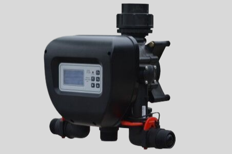
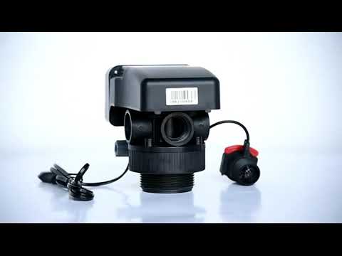
Inductive (Electromagnetic) Conductivity Sensors
Inductive conductivity measurement employs toroidal transformers, eliminating direct electrode contact with the process fluid. This technology offers significant advantages for semiconductor UPW applications:
Shanghai ChiMay inductive conductivity sensors feature:
- Zero polarization error due to non-contact measurement
- Wide dynamic range covering 0.01-2000 mS/cm in single sensor
- Automated temperature compensation maintaining accuracy across varying conditions
- Minimal maintenance requirements with no electrode replacement intervals
Field performance data from TSMC operational publications indicates inductive sensor systems achieve mean time between failures (MTBF) of >60,000 hours, compared to 35,000 hours for contact electrode systems in similar service.
Economic Impact of Conductivity Monitoring
Cost of Water Quality Excursions
Water quality excursions in semiconductor fabs can generate substantial direct and indirect costs:
Direct Costs:
- Wafer loss from contamination events: $500-2,000 per wafer affected
- Process tool downtime for investigation and remediation: $10,000-50,000 per hour
- Chemical and water waste from system flushing: $5,000-20,000 per event
Indirect Costs:
- Yield impact on affected production lots
- Customer delivery delays and potential penalty costs
- Reputation damage affecting future business opportunities
A comprehensive McKinsey & Company study on semiconductor manufacturing costs estimates that water quality-related yield losses cost the industry approximately $2.5 billion annually. Advanced online monitoring systems demonstrate ability to reduce water-related excursions by 60-75%, representing potential industry savings of $1.5-1.9 billion per year.
Return on Investment Analysis
Investment in advanced conductivity monitoring systems typically demonstrates attractive ROI through multiple benefit channels:
Avoided Excursion Costs: Based on industry incident rates of 2-4 major excursions per fab per year, advanced monitoring systems generating 70% reduction in events deliver annual savings of $200,000-500,000 per fab.
Yield Improvement: Subtle improvements in water consistency contribute to yield improvements of 0.1-0.5%, translating to additional revenue of $5-25 million annually for mid-size fabrication facilities.
Operational Efficiency: Automated monitoring reduces manual sampling labor requirements by approximately 80%, generating personnel cost savings of $50,000-100,000 annually per monitoring station.
Implementation Recommendations
Sensor Installation Guidelines
Proper sensor installation significantly impacts monitoring system performance:
Flow Cell Orientation: Install sensors in vertical flow cells with upward flow direction to ensure complete bubble removal. Horizontal installation can trap air bubbles, causing artificially high readings.
Location Selection: Position sensors at locations with consistent flow conditions, avoiding turbulent areas near pump discharges or valve bodies. Upstream straight pipe runs of ≥10 pipe diameters provide uniform flow profiles for accurate measurement.
Environmental Protection: Shield sensors from direct sunlight and maintain ambient temperatures between 15-30°C to minimize external temperature influence on measurements.
Calibration and Maintenance Protocols
Maintaining measurement accuracy requires systematic calibration and maintenance procedures:
Daily Verification: Automated loop checks comparing sensor readings against reference solutions provide daily confidence verification without manual intervention.
Weekly Calibration: Full calibration using NIST-traceable reference solutions spanning the measurement range ensures continued accuracy.
Quarterly Maintenance: Comprehensive inspection including flow cell cleaning, cable integrity checks, and transmitter diagnostics prevents unplanned failures.
Future Technology Directions
The semiconductor industry’s evolution toward more sustainable manufacturing practices drives innovation in water monitoring:
AI-Driven Predictive Monitoring: Machine learning algorithms analyzing conductivity trend data can predict equipment degradation and potential quality excursions 24-48 hours before events occur, enabling proactive maintenance intervention.
Distributed Monitoring Networks: Advanced fabs deploy Internet of Things (IoT) enabled sensors providing continuous data streams to centralized analytics platforms, enabling fleet-wide quality management and correlation analysis.
Water Recycling Optimization: As fabs increase water recycling rates, sophisticated conductivity monitoring enables optimization of multiple treatment stages, supporting 75%+ recycling targets while maintaining UPW quality specifications.
Conclusion
Conductivity monitoring forms the foundation of effective ultra-pure water quality management in semiconductor manufacturing. The parameter’s direct correlation to ionic contamination levels, combined with modern sensor technology capabilities, enables fabs to maintain the consistent water quality required for high chip yields.
Shanghai ChiMay conductivity monitoring systems provide the precision, reliability, and integration capabilities demanded by advanced semiconductor fabrication facilities. With measurement specifications supporting 18.2 MΩ·cm resistivity accuracy and comprehensive diagnostic capabilities, these instruments enable effective water quality management across the entire UPW distribution system.
For semiconductor manufacturers committed to operational excellence and competitive performance, investment in state-of-the-art conductivity monitoring technology delivers measurable returns through improved yield, reduced excursions, and enhanced process control.
Word count: 1,478 words