Semiconductor fabrication demands water purity levels exceeding virtually every other industrial application. Ultrapure water (UPW) serves as the primary raw material in chip manufacturing, contacting wafers during cleaning, rinsing, etching, and doping operations. Every contamination source threatens yield, making comprehensive water quality monitoring the foundation of successful semiconductor manufacturing. This guide presents the eight essential parameters that every semiconductor fab must monitor continuously.
Table of Contents
1. Resistivity: The Primary Purity Indicator
Resistivity measurement provides the fastest, most reliable indicator of ionic contamination in UPW systems. Pure water exhibits resistivity approaching 18.2 MΩ·cm at 25°C, with any dissolved ionic species causing measurable reduction. The ASTM D5127 guide establishes electronic-grade water specifications, while SEMI F63 defines requirements specifically for semiconductor processing applications—for its strictest line-width grades, SEMI F63 calls for inline resistivity of at least 18.18 MΩ·cm at 25°C.
Continuous resistivity monitoring enables real-time contamination detection, triggering alarms within seconds of quality degradation. Modern instruments achieve measurement accuracy of ±0.01 MΩ·cm at full scale, with temperature compensation ensuring consistent readings regardless of measurement conditions. Multi-point monitoring throughout the distribution system identifies contamination sources quickly, enabling rapid response before affected water reaches production equipment.
Shanghai ChiMay’s conductivity monitoring solutions include instruments specifically designed for semiconductor applications. These meters feature extended ranges up to 20 MΩ·cm, digital output for system integration, and diagnostic functions identifying sensor degradation before measurement accuracy suffers.
2. Total Organic Carbon (TOC): Preventing Organic Contamination
TOC measurement quantifies the total carbon content of organic compounds dissolved in UPW. Even trace organics can create defects through multiple mechanisms: photoresist interference, hydrophobic surface regions, and etch rate variations. The SEMI F63 specification limits TOC to 1 µg/L (1 ppb) for its most advanced grades, and cutting-edge fabs increasingly target sub-ppb control.
Online TOC analyzers employ UV oxidation combined with conductometric detection to achieve continuous measurement capabilities. Detection limits of 0.1 ppb or better enable reliable monitoring of water meeting stringent specifications. Sample handling requires careful attention— PTFE tubing and minimal dead volumes prevent organic leaching from sampling systems themselves.
3. Dissolved Oxygen (DO): Controlling Oxidation Potential
Dissolved oxygen concentration influences the oxidation-reduction environment during chemical processing steps. Many cleaning and etching processes depend on precise control of oxidation potential, which DO levels directly affect. Semiconductor-grade UPW typically maintains DO below 5 ppb, achieved through vacuum deaeration or nitrogen stripping systems.
Elevated DO can cause oxidation of metal surfaces within process chambers and distribution systems, generating particle contamination. Conversely, extremely low DO may inhibit certain chemical processes designed to operate under oxidative conditions. Continuous DO monitoring ensures consistent process chemistry throughout production operations.
4. Silica: Preventing Deposits on Wafers
Silica monitoring addresses a pervasive contamination challenge in semiconductor facilities. Silica originates from feed water dissolution of silicate minerals, from system components containing silicate materials, and from chemical-mechanical polishing operations in facilities performing backend processing. The SEMI F63 specification holds silica to sub-ppb concentrations for the advanced grades—published summaries of the standard cite roughly 0.1 µg/L for the strictest class—a level only reachable with careful pretreatment and monitoring.
Silica deposition on wafer surfaces creates defects that may escape detection until final testing, when yield losses become apparent. Sub-ppb silica analysis requires specialized techniques such as graphite furnace atomic absorption spectroscopy or ICP-mass spectrometry, as conventional analytical methods lack sufficient sensitivity for reliable measurement at specification levels.
5. Particle Counts: Maintaining Surface Purity
Particle monitoring protects wafer surfaces from contamination during water contact. As technology nodes advance, fabs monitor ever-smaller particles—down to tens of nanometers—with SEMI F63’s strictest grade holding particles at 20 nm and larger to roughly 1,000 per liter, about one particle per milliliter. The International Technology Roadmap for Semiconductors (ITRS), continued today as the IEEE International Roadmap for Devices and Systems (IRDS), has pushed these particle requirements tighter as nodes shrink.
Light-scattering particle counters provide continuous particle monitoring, detecting particles in flowing water without sample collection delays. Multiple size channels enable trend analysis and source identification when particle events occur. Monitoring points throughout the distribution system—including critical points-of-use—ensure comprehensive coverage of potential contamination sources.
6. pH: Maintaining Chemical Balance
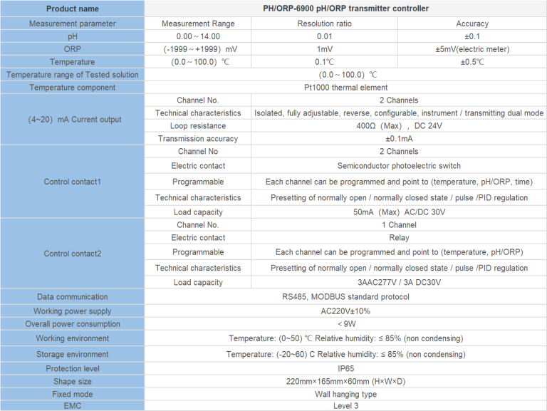
Although UPW’s extreme purity makes pH measurement challenging, pH monitoring provides useful information about system conditions and potential contamination. Neutral pH (7.0) indicates properly balanced water chemistry, while excursions in either direction signal potential contamination or system imbalances.
Traditional pH electrodes struggle with the low ionic strength of UPW, requiring specialized low-conductivity electrodes with rapid response times. Temperature compensation and careful electrode maintenance ensure reliable measurements. Shanghai ChiMay offers pH monitoring solutions designed for the challenging conditions of ultrapure water applications.
7. Temperature: Affecting All Process Parameters
Temperature monitoring supports accurate interpretation of all other water quality measurements. Resistivity, conductivity, and chemical reaction rates all vary with temperature, making compensation essential for meaningful data. Most semiconductor specifications reference measurements at 25°C, requiring automatic temperature compensation in monitoring instruments.
Temperature variations in distribution systems can cause localized condensation introducing contamination, while temperature gradients affect chemical reaction rates in process tools. Continuous temperature monitoring at critical points enables both measurement compensation and detection of abnormal thermal conditions.
8. Flow and Pressure: Ensuring Delivery Integrity
Flow and pressure monitoring ensure that water reaches process tools at appropriate conditions for effective operation. Insufficient flow can leave residue on wafer surfaces during rinsing operations, while pressure variations affect chemical delivery precision in process equipment.
Flow monitoring throughout the distribution system identifies blockages, leaks, and flow imbalance conditions affecting water delivery. Pressure transmitters at strategic locations ensure adequate pressure throughout the system while detecting abnormal conditions requiring intervention. Combined flow and pressure data enables predictive maintenance, identifying equipment degradation before failures occur.
Shanghai ChiMay: Your Complete Water Quality Monitoring Partner
Shanghai ChiMay delivers comprehensive water quality monitoring solutions addressing all eight critical parameters for semiconductor manufacturing. The product portfolio includes conductivity meters, TOC analyzers, particle counters, and multi-parameter monitoring systems designed for the demanding requirements of semiconductor fab operations.
Application engineering teams provide expert support for system design, sensor selection, installation, and ongoing calibration services. Shanghai ChiMay’s commitment to semiconductor industry excellence ensures reliable performance and accurate measurements throughout facility lifecycle. Partner with Shanghai ChiMay to implement world-class water quality monitoring protecting your manufacturing yield.