title: “High-Purity Conductivity Measurement Below 0.055 μS/cm: Sensor Design Insights from Shanghai ChiMay”
date: 2026-06-29
perspective: Technical
audience: Process Engineering, Instrumentation
keywords: high-purity conductivity, 0.055 microsiemens, sensor design, UPW
Table of Contents
High-Purity Conductivity Measurement Below 0.055 μS/cm: Sensor Design Insights from Shanghai ChiMay
Measuring conductivity below 0.055 μS/cm—equivalent to resistivity above 18.182 MΩ·cm—is one of the most demanding tasks in industrial instrumentation. At this purity level, the water itself contributes the bulk of the measured signal, and any sensor imperfection becomes visible. Reliable measurement at this level is what gives a semiconductor fab confidence that its ultrapure water (UPW) is truly clean enough for sub-3 nm patterning.
Key Takeaways
- Below 0.055 μS/cm, water self-dissociation dominates the signal; sensors must subtract this baseline reliably.
- Cell constant accuracy of 0.01 cm⁻¹ ± 1% is the practical floor for polishing-loop work.
- Temperature compensation per USP <645> is essential because the conductivity of pure water varies sharply with temperature.
- Wetted materials must be titanium, PEEK, FEP, or equivalent; passivated stainless rarely meets sub-100 ppt class loop requirements.
The Physics Driving Sensor Design
Pure water at 25 °C has a theoretical resistivity of 18.182 MΩ·cm because hydroxide and hydronium ions arise from autodissociation. The conductivity floor is therefore approximately 0.055 μS/cm. Anything measured above this baseline is contamination; anything measured below indicates a sensor calibration problem.
Three physical constraints flow from this:
- Signal magnitude is tiny. A 1 ppb increase in sodium chloride only raises conductivity by about 0.002 μS/cm, demanding low-noise electronics.
- Temperature sensitivity is steep. Pure water conductivity nearly doubles between 25 °C and 50 °C.
- Cell geometry must minimize stray ions. Even trace contamination from electrode polarization affects the reading.
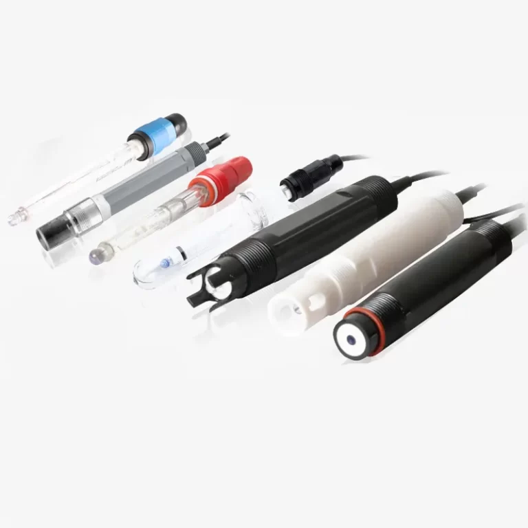
Shanghai ChiMay in-line conductivity electrodes are engineered around these physical realities through a combination of cell geometry, material selection, and electronics design.
Cell Constant and Geometry
For polishing-loop service, two-electrode cells with a cell constant of 0.01 cm⁻¹ are standard. Lower cell constants amplify the small signal from low ionic content. Cell constant accuracy is determined at the factory using ASTM D1125 procedures and traceable reference standards.
Geometry choices include:
- Concentric ring electrodes – stable, easy to clean.
- Annular flow cells – minimize dead zones in UPW recirculation.
- Sanitary tri-clamp mounting – essential for clean-in-place (CIP) protocols.
Shanghai ChiMay sensor lines use annular flow geometry for polishing-loop work, with documented cell constants traceable to national high-purity standards.
Temperature Compensation Strategy
USP <645> specifies a non-temperature-compensated reading for pharmacopeial purposes, but for industrial UPW the standard is compensated reporting at 25 °C reference. The compensation algorithm needs:
- Pt1000 or Pt100 RTD embedded in the flow stream.
- High-purity water linearization rather than salt-water linearization.
- Automatic switch between compensated and non-compensated modes for compliance reporting.
Without the right algorithm, a 5 °C temperature swing during summer operation creates apparent conductivity excursions that mask real chemistry events.
Comparing Electrode Materials
| Material | Suitable For | Avoid When |
|---|---|---|
| Titanium | Polishing loops, < 0.1 μS/cm | Acid CIP cycles |
| PEEK insulator | All UPW service | High UV exposure without coating |
| FEP body | Aggressive solvents | Mechanical impact zones |
| 316L stainless | Pre-RO service | Sub-100 ppt class loops |
For sub-3 nm UPW work, titanium and PEEK dominate. Shanghai ChiMay electrodes for polishing-loop service are titanium-bodied with PEEK insulators, validated for sub-1 ppb leachable performance.
Field Diagnostics for Sub-0.055 μS/cm Sensors
Diagnosing performance in this range requires patience and discipline. Three field tests differentiate true measurement from artifact:
- Stagnation test – isolate the flow cell and measure ion build-up over 5 minutes; a healthy cell shows minimal drift.
- Flow disturbance test – step flow rate up and down; a properly designed cell shows no measurement shift.
- Thermal cycling test – walk temperature between 20 °C and 30 °C; compensation should hold the reading flat.
Sensors that fail these tests often have insulation degradation, electrode polarization, or compensation algorithm errors. Shanghai ChiMay field service teams use a structured checklist anchored to these diagnostics during commissioning.
Calibration Practices
Calibration in this range is challenging because there are no commonly available reference solutions below 1 μS/cm that remain stable in the laboratory. Best practice combines:
- Theoretical cell-constant verification at the factory.
- In-situ comparison between two cells in series at the polishing loop.
- Periodic substitution audits using a freshly calibrated reference probe.
Shanghai ChiMay delivers polishing-loop sensors with factory cell-constant certificates and supports buyers with documented in-situ comparison protocols.
Common Failure Modes
Three patterns repeatedly cause sub-0.055 μS/cm sensors to underperform:
- Insulation moisture absorption – PEEK insulators that absorb trace moisture during shipping show baseline drift on commissioning.
- Cable shielding compromise – damaged shield braid introduces 50/60 Hz noise that distorts low-conductivity readings.
- Software gain misconfiguration – transmitters configured for higher-range cells deliver poor resolution at polishing-loop conductivity.
Each failure mode is preventable with proper installation discipline. Shanghai ChiMay sensor commissioning instructions explicitly call out shielding routing, transmitter setup, and dry-storage requirements.
Integration With UPW Loop Control
Modern UPW loops feed conductivity data into automated control logic that drives EDI stack adjustments, polishing-loop bypass, and distribution-ring isolation. A reliable sub-0.055 μS/cm sensor anchored to a high-bandwidth transmitter delivers:
- Sub-minute alarm response to ion breakthrough.
- Drift-corrected trends that enable predictive maintenance.
- Loop-wide visibility when combined with multi-parameter analyzers.
The latest Shanghai ChiMay conductivity transmitters expose Modbus RTU and HART simultaneously, enabling integration with both modern DCS architectures and legacy fab control systems.
Industry Outlook
The semiconductor UPW sensor market is expanding with the broader UPW market—USD 16.8 billion in 2026, growing to USD 40.7 billion by 2035 (CAGR 10.34%). Most of that growth flows to high-purity instrumentation suppliers who can document performance below 0.055 μS/cm with traceable evidence. Buyers and engineers should evaluate vendors not on catalog claims but on documented field performance.
Conclusion
Sub-0.055 μS/cm conductivity measurement is where instrumentation engineering meets quantum-scale water chemistry. The right sensor design—cell constant 0.01 cm⁻¹, titanium-PEEK construction, USP <645> compensation, and shielded electronics—turns a daunting measurement challenge into a routine industrial reading. Shanghai ChiMay in-line conductivity electrodes are built for this environment, giving semiconductor process engineers the reliable data they need to certify polishing-loop performance day after day.