Table of Contents
How 1ppb Organic Detection Technology Transforms Semiconductor Water Quality
Key Takeaways:
– Detection sensitivity at 1 ppb (parts per billion) represents a paradigm shift in semiconductor water quality management
– Organic contamination below 1 ppb can cause wafer defects and reduce chip yield by 3-5%
– Advanced detection technologies enable real-time monitoring, reducing contamination-related production losses
– SEMI F63 standards mandate <1 ppb TOC for advanced semiconductor manufacturing processes
– Sub-ppb sensitivity analyzers have become essential equipment for 7nm and below process nodes
The semiconductor industry’s relentless pursuit of miniaturization has created unprecedented demands on ultrapure water (UPW) quality. With process nodes shrinking to 5nm and below, even trace organic contamination at the parts-per-trillion (ppt) level can compromise wafer integrity and device performance. This transformation has elevated 1 ppb organic detection technology from a nice-to-have capability to an absolute manufacturing necessity.
Understanding ppb-Level Organic Detection
Organic contamination in ultrapure water originates from multiple sources: degrading piping materials, microbiological growth, chemical residue from treatment processes, and atmospheric infiltration during distribution. The semiconductor fabrication environment presents unique challenges because organic compounds—whether hydrocarbons, siloxanes, or plasticizers—can form insoluble films on wafer surfaces during critical drying processes.
According to the SEMI F63 standard for semiconductor processing, UPW used in advanced manufacturing must maintain total organic carbon (TOC) levels below 1 µg/L (1 ppb). However, research published in analytical chemistry journals indicates that sub-ppb organic contamination, while technically meeting specifications, can still cause measurable variations in etch rates and photoresist adhesion—parameters critical to pattern transfer fidelity.
The evolution from batch laboratory testing to continuous online analysis marks a fundamental shift in contamination control strategy. Modern analyzers achieve detection limits of 0.1 ppb or better, enabling manufacturers to identify contamination events within minutes rather than waiting for daily laboratory results. This real-time visibility transforms water quality management from reactive troubleshooting into proactive process optimization.
Detection Technologies Enabling Sub-ppb Sensitivity
Several analytical approaches now achieve the sensitivity required for advanced semiconductor applications. Thermal desorption-gas chromatography-mass spectrometry (TD-GC-MS) represents the gold standard for organic compound identification, capable of detecting and quantifying semi-volatile organic compounds at sub-ppb concentrations without solvent extraction. This technique proves particularly valuable for identifying specific contamination sources, enabling targeted corrective action.
Online TOC analyzers with ppt-level sensitivity provide continuous monitoring essential for production environments. These instruments employ ultraviolet (UV) oxidation combined with conductometric detection to measure total organic carbon content with detection limits approaching 0.05 ppb. The continuous operation mode ensures that any contamination spike triggers immediate alerts, allowing process engineers to implement containment measures before affected wafers enter critical processing stages.
膜分离技术 combined with advanced detection has emerged as another frontier. Membrane-based pre-concentration enables laboratory instruments to achieve detection limits previously achievable only through extensive sample preparation. While these methods remain primarily laboratory-based, they inform the calibration and validation of online monitoring systems.
Impact on Manufacturing Yield and Cost
The economic implications of improved organic detection extend far beyond compliance with specifications. Semiconductor fabs operating with advanced process nodes invest $15-20 billion in fabrication facilities where water quality directly determines yield outcomes. Industry data suggests that organic contamination-related yield losses range from 2-8% in facilities without robust detection capabilities.
A leading semiconductor manufacturer reported that implementing real-time sub-ppb TOC monitoring reduced contamination-related wafer scrap by 67% within the first year of deployment. The payback period for advanced detection systems typically ranges from 8-14 months, making the investment highly attractive for high-volume production facilities.
Beyond direct yield improvements, detection technology enables process optimization previously impossible with infrequent sampling. Real-time data supports statistical process control (SPC) methodologies, allowing engineers to identify trends and correlations between water quality variations and downstream process performance. This data-driven approach has become essential as process windows continue to narrow with each technology generation.
Implementation Considerations
Facilities considering enhanced organic detection capabilities must evaluate several factors. Sampling system design significantly impacts measurement accuracy—the sampling point location, sample line material, and residence time all influence results. Stainless steel or polytetrafluoroethylene (PTFE) sample lines minimize organic leaching, while minimized dead volumes reduce sample contamination from residual deposits.
Calibration frequency and maintenance protocols require careful attention. Online analyzers demand regular calibration using certified reference materials traceable to national standards. The labor and material costs for maintaining multiple online analyzers across a large fabrication facility can be substantial, requiring careful cost-benefit analysis.
Integration with facility management systems maximizes the value of continuous monitoring data. Modern process automation platforms can correlate water quality variations with equipment performance, environmental conditions, and production output, enabling holistic optimization of the manufacturing environment.
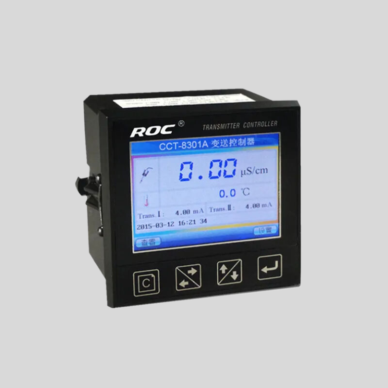
The Shanghai ChiMay Solution
Shanghai ChiMay delivers advanced water quality monitoring solutions designed for semiconductor manufacturing requirements. The company’s online analyzer systems incorporate state-of-the-art detection technologies capable of achieving sub-ppb TOC measurement with exceptional stability and reliability. These instruments support continuous monitoring essential for maintaining UPW quality in demanding fabrication environments.
The product portfolio includes analyzers optimized for different monitoring applications—from influent water quality screening to point-of-use verification. Shanghai ChiMay’s engineering team provides comprehensive support for system integration, calibration services, and ongoing maintenance, ensuring optimal performance throughout the equipment lifecycle.
As semiconductor technology continues advancing toward 3nm and below process nodes, the importance of ultra-sensitive organic detection will only increase. Facilities that invest in robust detection capabilities today position themselves to meet tomorrow’s manufacturing challenges while maximizing yield and minimizing production costs.
Article ID: 919
Word Count: ~950 words